Part one ended with a slab of the purest material in industry, grown as one crystal, polished flatter than almost anything else made, with a precisely measured trace of boron or phosphorus patterned into it.
It could not compute anything. This is the part where it starts to.
I am going to build up from one atom to a sandboxed process without skipping a rung, because circuits are a black box for most people and the box only opens if nothing is hand-waved. The physics stays light. Everything here is a switch, and then a lot of switches.
What doping actually does
A silicon atom has four outer electrons. In the crystal, each one bonds to four neighbours, and every electron is accounted for. There is nothing loose. That is precisely why pure silicon barely conducts: conduction needs charge that is free to move, and in a perfect silicon lattice there is none.
Now swap one atom in ten million for phosphorus, which has five outer electrons. Four of them take up bonding duty like everyone else. The fifth has nothing to do and drifts free. Do that a few billion times and you have a material with mobile negative charge in it. That is n-type silicon.
Swap in boron instead, which has three. Now there is a bond missing an electron, and that gap is called a hole. An electron from a neighbouring bond slides over to fill it, which leaves a gap where that electron came from, and so on. The electrons shuffle one way and the gap appears to travel the other way, like the one empty space in a full car park moving around as people shuffle into it. That is p-type silicon, and the mobile charge behaves positive.
A hole is not a particle. It is bookkeeping, and it is much easier to track one gap than the thousands of electrons taking turns to fill it.
Two kinds of dirt, side by side
Put n-type next to p-type in the same crystal and something happens on its own. Free electrons on the n side wander across, meet holes on the p side, and cancel out. The region right at the boundary empties of mobile charge and becomes an insulator, and the atoms left behind, now unbalanced, set up an electric field across that gap.
That field pushes back. It reaches an equilibrium, and the result is a junction that conducts in one direction and not the other. Push current the way the field opposes and nothing happens. Push it the other way and the barrier collapses and current flows.
That is a diode. A one-way valve for electricity, made from nothing but one crystal contaminated two different ways.
The switch, and the thing everyone gets wrong about it
Now the important one.
Start with p-type silicon. Make two n-type islands in it, a little apart. Call them source and drain. Between them sits p-type material, so going source to drain you cross two junctions pointing opposite ways. Whichever direction you push, one of them blocks. No current. Off.
Now lay a thin insulator over the gap, and a conductor on top of that. The conductor is the gate.
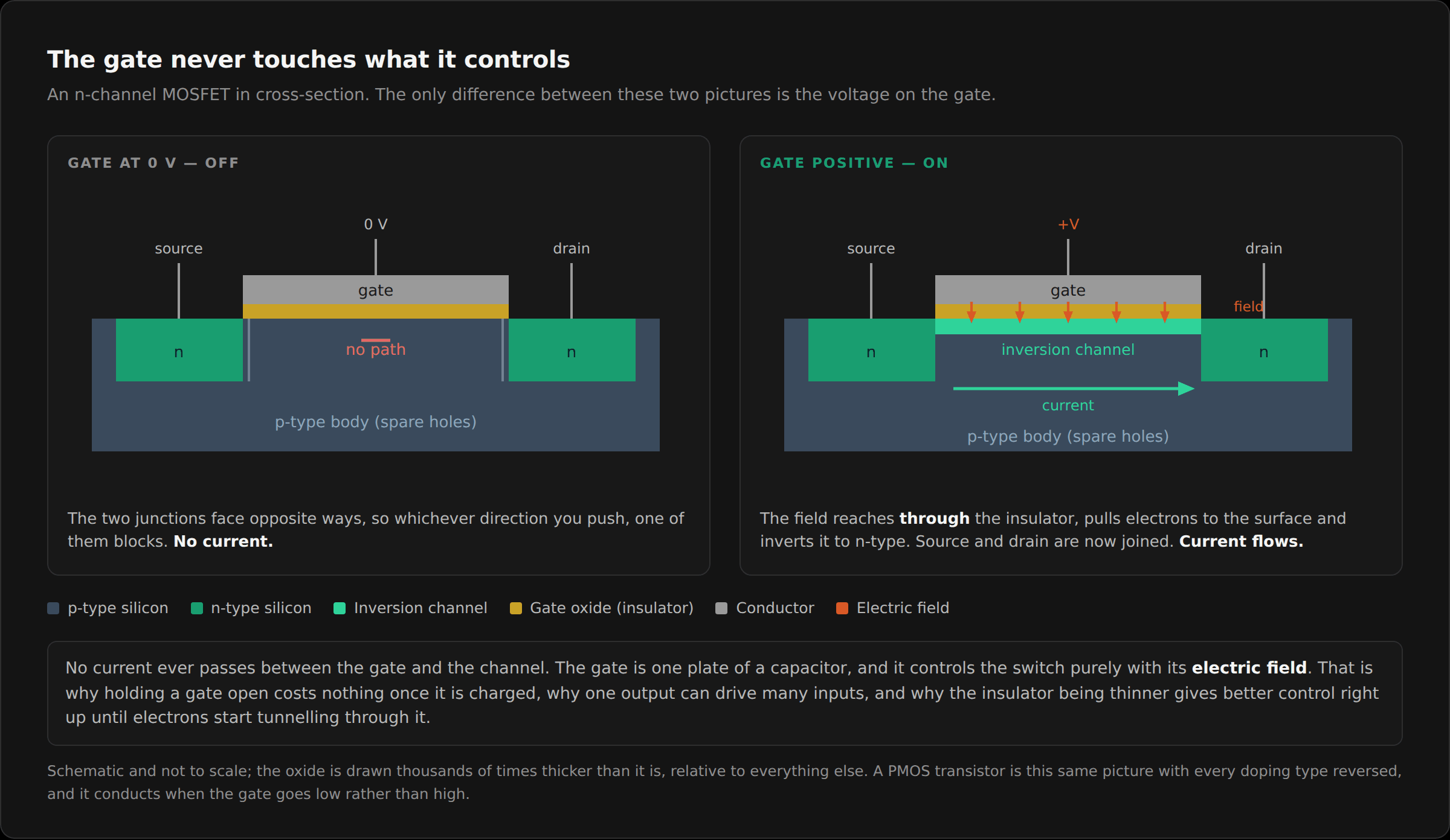
Here is the part that surprises people, and it is the single most important fact in this whole essay: the gate does not touch anything it controls. It is separated from the silicon by an insulating layer, and it is supposed to be. No current flows from the gate into the channel. It is one plate of a capacitor.
What it does instead is make a field. Put a positive voltage on the gate, and that field reaches through the insulator into the p-type silicon below, pushing holes away and pulling the few loose electrons up toward the surface. Turn it up enough and the surface layer stops behaving p-type at all. It inverts, becoming effectively n-type, and now there is a continuous n-type path from source to drain.
Current flows. On.
Drop the gate voltage, the field disappears, the channel evaporates, and you are back to two opposed junctions. Off.
Three consequences fall out of that, and each one matters later.
The gate draws essentially no steady current. You pay to charge the capacitor and then it sits there. This is why one output can drive a great many inputs, and it is the foundation of everything above.
Thinner insulator means better control, because the same voltage makes a stronger field across a shorter distance. That pressure is why the oxide got so absurdly thin, which is where part one's scale ladder ended up: down around twice the spacing of the silicon lattice. It stopped there because below that, electrons simply tunnel straight through the insulator, and a switch that leaks when it is off is not much of a switch.
Silicon won partly because of rust. Heat silicon in oxygen and it grows its own oxide, and silicon dioxide happens to be a superb insulator that bonds cleanly to the crystal beneath it. Germanium is a better semiconductor in several respects, but its oxide is soluble in water. The material that won is the one whose native corrosion product happened to be glass.
Two flavours, and why that is the whole trick
Build that device with n-type source and drain in a p-type body and you get an NMOS transistor: it turns on when the gate goes high.
Build the mirror image, p-type source and drain in an n-type body, and you get a PMOS transistor: it turns on when the gate goes low.
One is on when the other is off. Wire them as a complementary pair and you get the arrangement that the entire industry is named after.
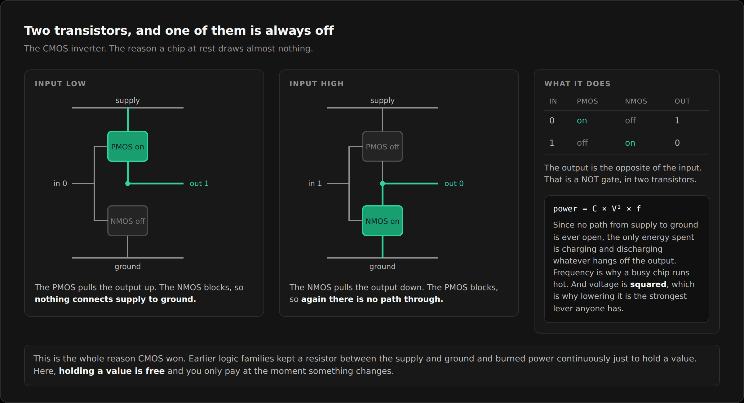
Put a PMOS between the supply and the output, an NMOS between the output and ground, and tie both gates to the same input.
Input high: the NMOS conducts and the PMOS blocks, so the output is pulled down to ground. Output low.
Input low: the PMOS conducts and the NMOS blocks, so the output is pulled up to the supply. Output high.
The output is the opposite of the input. It is a NOT gate, and it is two transistors.
But look at what is not happening. In either resting state, exactly one of the two is off, so there is no path from the supply to ground. A CMOS gate sitting still draws almost nothing. You only pay when it switches, because switching means charging or discharging the capacitance hanging off the output.
That gives the relationship that governs every power budget in computing:
switching power = capacitance x voltage squared x frequency
Frequency is why a busy chip is hotter than an idle one. Capacitance is why smaller is cheaper to run. And voltage is squared, which is why dropping the supply voltage is the single most effective lever anyone has, and why chips run at a fraction of a volt rather than the five volts older parts used.
Four transistors, and then everything
Add one more of each and you get the gate that matters most.
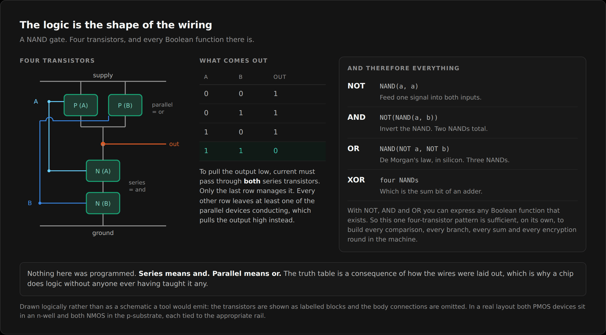
Two NMOS in series from the output down to ground. Two PMOS in parallel from the supply down to the output.
For the output to be pulled low, current has to get through both NMOS devices, one after the other. That needs input A high and input B high. Any other combination breaks the chain, and meanwhile at least one of the parallel PMOS devices is conducting, so the output gets pulled high instead.
The output is low only when both inputs are high. That is NAND, and notice that the logic is not programmed into it. The logic is the shape of the wiring. Series means and. Parallel means or.
Then comes the fact that makes the whole discipline possible. NAND is functionally complete. Feed the same signal into both inputs and you get NOT. Invert a NAND and you get AND. Invert both inputs of a NAND and you get OR. From those three you can construct any Boolean function whatsoever.
Every comparison, every branch, every piece of arithmetic, every pixel, every encryption round, is that one four-transistor pattern repeated.
Arithmetic is a shape of wire
Take two bits and ask for their sum.
The result bit is 1 when exactly one input is 1, which is XOR. The carry bit is 1 when both are 1, which is AND. Two gates, and you have added two bits. That is a half adder.
Add a third input so it can accept a carry coming in from the column to its right, and it becomes a full adder. String thirty two of them together, each one handing its carry to the next, and you have a machine that adds thirty two bit numbers.
Subtraction needs no new hardware: flip every bit and add one, and addition does the rest. Multiplication is shifting and adding. Comparison is subtraction where you only keep the flags.
The thing worth taking from this is that arithmetic is not a special faculty the chip has. It is what falls out when you wire switches in a particular shape. Nobody taught it to count.
Holding still, and the drumbeat
Everything so far has no memory. The output of a NAND gate is a function of what its inputs are doing right now, and if the inputs change the output follows.
Cross-couple two inverters, output of each into the input of the other, and something different happens: the pair has two stable states and will sit in whichever one it was put into. That is one bit, held. Add a little gating so it only accepts a new value when told to, and you have a flip-flop.
Now add the clock, which is the drumbeat the whole chip marches to.
Between two ticks, signals ripple through the combinational logic and settle. On the tick, every flip-flop captures whatever has settled at its input. Which means the clock period has to be longer than the slowest path through the logic. That slowest path is the critical path, and it is what actually sets the maximum clock speed of a design. Not marketing. The propagation delay of the worst chain of gates on the chip.
Registers holding state, logic computing the next state, a clock deciding when. That is a state machine, and a processor is a large and very specific one.
From switches to instructions
Wire up some flip-flops into registers. Wire up adders and logic gates into an arithmetic unit. Then add a block whose job is to take a number and turn it into control signals: which register feeds the adder, whether to add or subtract, where the answer goes.
That block is the instruction decoder, and it means an instruction is literally just a number. Feed the right pattern of bits in and the right switches open and close.
The instruction set architecture is the contract that names those patterns. This bit pattern means add these two registers. That one means load from this address. Everything above this point, all of it, depends on that contract being kept.
And here is the subtlety that pays off at the end. The contract says nothing about how. A modern processor does not execute instructions one at a time in order. It overlaps them, reorders them, and guesses which way a branch will go so it can start work before it knows. It is allowed to do all of that, so long as the result it presents matches what the contract promised.
A stack of promises
On top of the ISA, every layer is a boundary that exists because the layer below it agreed to hold something in.
Machine code gets generated by a compiler, so you can write in something humane. The operating system gives every process the convincing illusion that it owns the whole machine. That illusion is enforced in hardware by the memory management unit, which translates the addresses a program uses into real ones, and simply refuses to translate addresses belonging to anyone else. A pointer in one process cannot name memory in another, because the hardware will not let it resolve.
Above and below that sit more of the same. Privilege levels keep user code from executing instructions only the kernel may run. A hypervisor does to operating systems what an operating system does to processes. A container, a VM, a browser tab, a sandbox: each one is a promise that what is inside cannot reach what is outside.
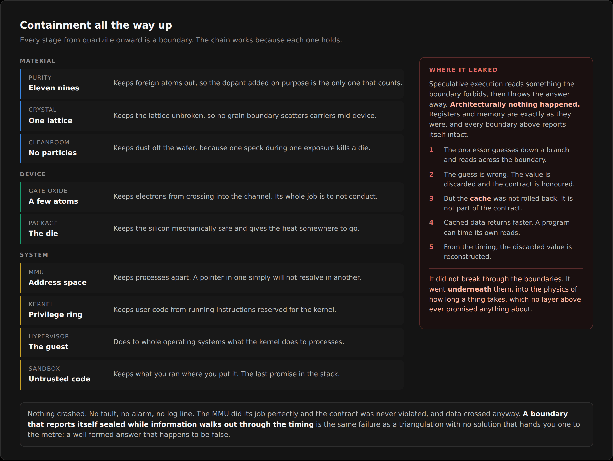
That is the whole picture, and it is the reason for the title. Every stage from quartzite onward has been about keeping something out or keeping something in. Eleven nines of purity to keep foreign atoms out. One continuous crystal to keep the lattice from breaking. A cleanroom to keep particles off the wafer. A gate oxide a few atoms thick whose entire job is to not conduct. A package to keep the die safe. An MMU to keep processes apart. A sandbox to keep untrusted code where you put it.
Sand to sandbox. It is containment all the way up.
Where it leaks
Which brings us to the interesting failure.
Remember that the processor is allowed to guess. It speculates down a branch, and if the guess was wrong it throws away the results. Registers and memory are restored. The contract is honoured exactly: architecturally, nothing happened.
But something did happen. The speculative work touched the cache, and the cache was not rolled back. It had no reason to be, because the cache is not part of the contract. It is an implementation detail, invisible by definition.
Except it is measurable. Data that is in cache comes back faster than data that is not, and a program can time its own memory accesses. So you convince the processor to speculatively read something it should not, note that it discards the value, and then work out what that value was by timing which cache lines are now warm.
The boundary held at the level it promised to hold. It leaked one level down, in the physics of how long a thing takes.
Nothing crashed. There was no error, no fault, no alarm. The MMU did its job perfectly, the ISA contract was never violated, and data crossed a boundary that every layer above reported as intact.
I have written about this shape three times now in systems that have nothing to do with each other. A contract address sitting in a table, authoritative-looking, returning a real balance under a confident wrong label. A honeypot field that caught real customers and answered every one of them with a success message. A triangulation with no valid solution that hands you one anyway, to the metre.
And now a containment boundary that reports itself sealed while information walks out through the timing.
Every one of them returns a well formed answer that happens to be false. The fix is always the same and it is always the hard part: work out what the failure actually looks like from the inside, and make the system capable of saying so.
The short version
Sand is silicon dioxide. Burn the oxygen off and you have silicon that is far too dirty. Turn it into a liquid so you can distil it, then turn it back into a solid, and now it is clean to a hundred billion to one. Melt it and pull one enormous crystal out of the melt so the lattice never breaks. Slice it, polish it flatter than almost anything, and photograph patterns onto it a few dozen times, using light to decide where a stencil lets you etch and where you drive in exactly the contamination you removed.
Do that and you have regions of silicon with spare electrons and regions with spare gaps. Put them next to each other and you have a valve. Hang an insulated plate over the gap and you have a switch that costs nothing to hold open. Wire four switches in a particular shape and you have a gate that can build any logic there is. Wire those into adders and latches, march them to a clock, and give the patterns names.
Then build fifty years of abstraction on top, every layer trusting the one beneath it to hold the line.
It is rock, all the way down. We just organised it very carefully and then agreed to believe in the organisation.
Climb it in GregTech
GregTech, a tech mod for Minecraft, has its own version of this climb. Its circuits come in voltage tiers, and each tier lines up with a step in this essay: a switch, then logic, then arithmetic, then memory, then instructions, and at the top, the sandbox. Go up the ladder one rung at a time. Each rung shows what the game makes, what it stands for in a real chip, and a button to build it or run the machines.
The recipes come from GregTech CEu Modern 7.5.3 and the TerraFirmaGreg modpack, read from their source files. The game side has its own notes: GregTech's first two circuits and real chips are crystals too.
Gunnar
Founder, Tofte Ventures LLC