Correction, 28 September 2026. Four parts here were first called by the names in GregTech's code and tooltips rather than the names the game shows. The LV processor is the Microchip Processor (the Microprocessor is GregTech's MV circuit), the CPU is the CPU Chip, the nanocomponent CPU is the Nano CPU Chip, and the Elite Circuit Board is the Multi-layer Fiber-Reinforced Printed Circuit Board, whose tooltip calls it an elite board. The names are from the pack's own English file. No number changed.
GregTech has crystal processors: chips grown from an emerald in an autoclave, fired at 5,000 K, and engraved with a laser. It sounds like fantasy. The real version is closer than it looks, because nearly every chip you have ever used is already a crystal.
This post goes through three things. How real chips come out of a crystal, and how TerraFirmaGreg copies it. What crystals can store. And what a system on a chip is, in the real world and in GregTech. Then you can run the components through the machines yourself.
A chip starts as a crystal
A chip starts as a single crystal of silicon: one continuous lattice, the size of a log. It is grown by the Czochralski process. High-purity silicon is melted in a quartz crucible at about 1,412°C. A small seed crystal, about 5 mm across, is dipped into the melt and pulled slowly out, and the silicon freezes onto it in the seed's own lattice. The finished crystal can be 300 mm across and weigh up to 1,000 kg. It is sliced into wafers, and the chips are made on the wafers. That makes Czochralski silicon the main substrate of the semiconductor industry.
The silicon going into that crucible has to be very pure first. The usual route is the Siemens process. Silicon reacts with hydrogen chloride to make trichlorosilane, which is distilled. The trichlorosilane then breaks down at about 1,050 to 1,150°C and deposits pure silicon onto heated silicon filaments, which grow into rods 15 to 20 cm thick.
TerraFirmaGreg builds this almost step for step. Its scripts turn silicon dust, hydrochloric acid and hydrogen into chlorosilanes, then silane, then polysilicon. They grow a silicon seed crystal in an autoclave and make a quartz crucible in an arc furnace. Then the High Temperature Precision Fabricator pulls a "Monocrystalline Silicon Boule" from 32 ingots' worth of molten polysilicon, with the seed and a pinch of gallium arsenide. The crucible is used up one run in twenty.
The boule needs a furnace rated for 1,784 K, which is about 1,511°C, a hundred degrees over the melt temperature above. Plain GregTech makes its boule in a blast furnace from silicon dust; TerraFirmaGreg removes that recipe and uses its own.
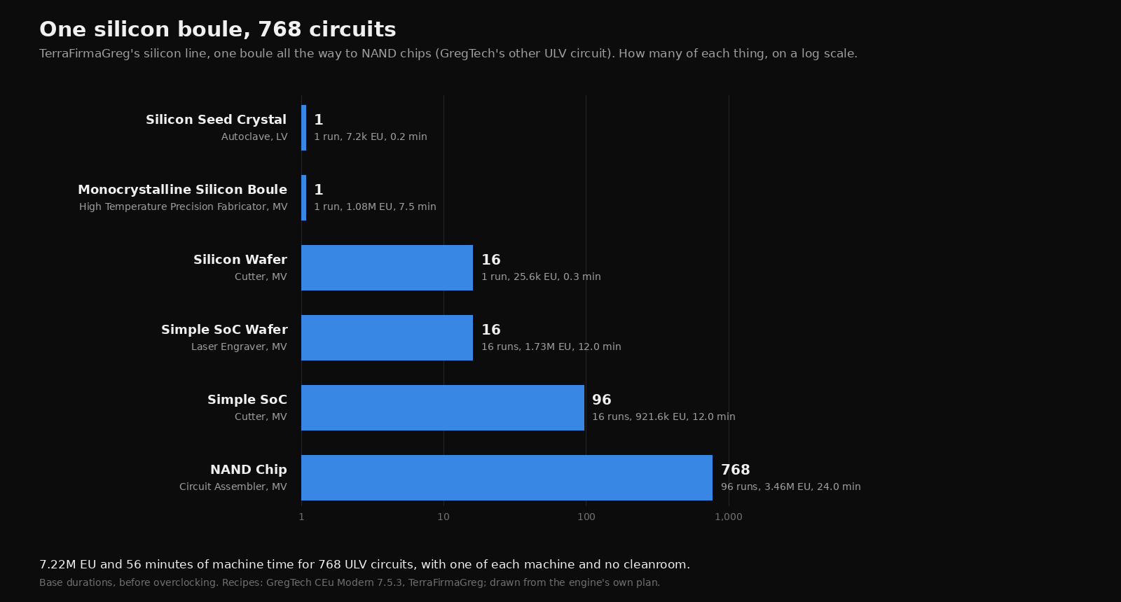 One boule planned all the way down to NAND chips. Drawn from the engine's own plan.
One boule makes 768 NAND chips. It is cut into 16 wafers. Each wafer is laser-engraved into a Simple SoC wafer and cut into 6 Simple SoCs, and each SoC makes 8 NAND chips. A NAND chip is GregTech's other ULV circuit, the same tier as the vacuum tube. The whole line is 7.22 million EU and 56 minutes of machine time, with no cleanroom needed.
That works out to about 9,400 EU per NAND chip, against 1,547 EU for a vacuum tube made on machines. So the silicon circuit costs six times the power. What it saves is the parts: no resistors, no glass tubes, no hand work. It is the first sign of what the rest of GregTech does, which is swap parts for power.
What crystals can store
"Crystal storage" covers several very different things, and some of them are not crystals at all.
- The "5D memory crystal" is glass. Researchers at the University of Southampton write data into fused silica with a femtosecond laser. Each nanostructure stores bits in its size and orientation as well as its three-dimensional position. They report 360 TB per disc, stability to 1,000°C, and a lifetime of 13.8 billion years at 190°C. The press calls it the "Superman memory crystal". But fused silica is amorphous: its atoms have no long-range order, unlike quartz, which is the same compound as a crystal.
- Microsoft's Project Silica is glass too. Its 2025 paper in Nature reports 4.8 TB in a 120 × 120 × 2 mm piece of fused silica. That is 301 layers at 1.59 gigabits per cubic millimetre, written at 25.6 megabits a second per laser beam. The suggested lifetime is over 10,000 years. A cheaper borosilicate version holds 2.02 TB.
- Diamond is a real crystal that stores bits. A group at City College of New York used nitrogen-vacancy defects in diamond as memory. Each bit is an atom-sized defect that traps or releases an electron when a laser hits it. They reached a two-dimensional density comparable to a DVD, rewritable, with virtually no loss of data over time if kept in the dark.
- Lithium niobate stores holograms. An iron-doped lithium niobate crystal holds data as an interference pattern through its whole volume. It has been studied for decades: large crystals, long storage lifetimes, strong diffraction. Its slow response is what has kept it out of products.
- In phase-change memory, the bit is whether it is a crystal. A chalcogenide such as germanium-antimony-tellurium switches between a crystalline and an amorphous state in under 100 nanoseconds. The two states differ in resistance by about three orders of magnitude, so crystal is one value and glass is the other. This is the closest thing on the list to "storing information in a crystal", and it is the working principle of a real memory technology.
- Ferroelectric RAM stores bits in which way a crystal points. A ferroelectric such as lead zirconate titanate (PZT) has two polarisation states that stay put when the power is off. One is a 1 and the other a 0.
- A quartz crystal keeps the time, not the data. Quartz is piezoelectric, so a voltage makes it vibrate. A watch crystal vibrates 32,768 times a second, which is 2 to the 15th. That way a 15-bit counter overflows exactly once a second.
I read these through search results, not the full papers. The numbers are the researchers' own claims as reported.
What a system on a chip is
A computer used to be a board of separate chips: the processor, the graphics, the memory controller, the input and output, each its own package, wired together through the board. A system on a chip puts all of those on one piece of silicon. It is faster, because signals do not have to leave the chip. It uses less power and less space, which is why phones are built around them.
GregTech models exactly that trade. Its LV processor, the Microchip Processor, has two recipes:
- From parts: a plastic board, a CPU Chip, 2 resistors, 2 capacitors, 2 transistors and 2 fine copper wires make 3 Microchip Processors. It takes 10 seconds at 60 EU/t, which an MV circuit assembler can run.
- From a system on a chip: a plastic board, one SoC, 2 fine copper wires and 2 tin bolts make 6 Microchip Processors. It takes 2.5 seconds at 600 EU/t, in a cleanroom.
The SoC replaces the CPU Chip and all six discrete parts, doubles the output, and makes each chip eight times faster (8.3 ticks against 66.7). It also takes a quarter more energy per chip at the assembler (5,000 EU against 4,000), and 600 EU/t is past HV's 512. So, made this way, an LV circuit needs an EV machine and a cleanroom. That is the real bargain in miniature: integration is cheaper in parts and dearer in fabrication.
GregTech's crystal chip
The crystal line is GregTech's own. TerraFirmaGreg changes only the solder on its circuits.
Growing the chip. An exquisite emerald or olivine goes into an autoclave with 16 mB of molten europium, a ninth of an ingot, in a cleanroom. Ten minutes later there is a one-in-four chance of a raw crystal chip. Then comes the loop. A forge hammer breaks one chip into 9 parts, and each part goes back into the autoclave with another 16 mB of europium to grow into a whole chip. One chip becomes nine. Three rounds turn one chip into 729.
That loop is the part of GregTech's crystal that echoes the real thing: every chip grows from a piece of an earlier one, the way a boule is pulled from a seed. And it is much cheaper than the emerald:
- From an emerald: 4 exquisite emeralds, 64 mB of europium, 15.4 million EU and 40 minutes of autoclave time per chip, on average.
- Grown from parts: 18 mB of europium, 6.49 million EU and 11 minutes of autoclave time per chip.
Firing and engraving. The raw chip goes into the electric blast furnace with an emerald plate and 1,000 mB of helium, at 5,000 K. A laser engraver with a lime lens turns it into a Crystal CPU, at 10,000 EU/t, which needs a LuV machine. A second engraving with a blue lens turns the CPU into a Crystal SoC, at 40,000 EU/t. That is past LuV's 32,768, so it needs a ZPM laser engraver.
The processor. The Crystal Processor is an IV circuit, and it has the same two recipes as the Microchip Processor:
- From parts: a Multi-layer Fiber-Reinforced Printed Circuit Board, a Crystal CPU, 2 Nano CPU Chips, 6 advanced SMD capacitors, 6 advanced SMD transistors and 8 fine niobium-titanium wires make 2 processors, at 9,600 EU/t. That is already a LuV machine: the IV circuit cannot be made on IV power.
- From the Crystal SoC: the board, the SoC, 8 fine niobium-titanium wires and 8 yttrium barium cuprate bolts make 4 processors, at 86,000 EU/t, a ZPM machine.
Counted in the energy this engine can see, the SoC route is not cheaper: about 5.13 million EU a processor against 4.92 million from parts. What it saves is the parts. No Nano CPU Chips, no SMD capacitors or transistors, each of which has a production line of its own that this engine does not follow. It is the Microchip Processor's trade again, a few tiers up.
Could a crystal board run a chip?
Not the way GregTech's name suggests. In GregTech the crystal is the chip, not the board: the Crystal Processor sits on a Multi-layer Fiber-Reinforced Printed Circuit Board, which its tooltip calls an elite board, like any other circuit of its era.
A board also does not run a chip. It carries power and signals between chips. The computing happens in the chip's own crystal layer. But real chips are built on specialised crystal substrates, for two reasons:
- Sapphire for isolation. Silicon on sapphire grows a thin layer of silicon on a single crystal of sapphire. The sapphire insulates, which removes the stray capacitance of a silicon base. That suits radio-frequency switches and amplifiers, and it is valued in military and aerospace work because it is radiation hardened.
- Diamond for heat. Single-crystal diamond conducts heat at up to 2,400 W/mK, against 40 to 400 W/mK for sapphire, silicon carbide and silicon. In early simulations that paper reports, putting gallium nitride transistors directly on diamond lowered their junction temperatures by 25 to 50 percent. The hard part is joining two crystals whose lattices do not match.
The newest "crystal board" is not a crystal. Intel announced glass core substrates in September 2023, planned for later this decade. It says they could allow up to ten times the interconnect density of today's organic packages. Glass, like the 5D memory, is amorphous.
So the honest version of "a specialised crystal board running a chip" is sapphire or diamond under a thin crystal of silicon or gallium nitride. It exists, it is used where isolation or heat matters, and the chip is still the crystal on top.
The check
The engine's recipe rows went from 38 to 71. Every one is read from GregTech CEu Modern 7.5.3, TerraFirmaGreg's scripts, or its core mod, at the version the pack pins. A script reads each row back out of those files and checks its timing, power and source. It also now checks the inputs GregTech's recipe types add after a recipe is written:
- The circuit assembler adds solder: 144 mB of tin, plus a copy of the recipe with 72 mB of soldering alloy. TerraFirmaGreg swaps those by tier: soldering alloy and Wood's metal at MV and HV, Wood's metal and a six-metal solder from EV up.
- The cutter adds lubricant, plus a water copy at twice the time and a distilled-water copy at one and a half.
Missing the first of these was an error in the circuit post, which now carries a correction. It changed no copper or energy figure there.
The crystal loop has no end, so the planner cannot walk it. The engine carries its steady state as a derived recipe, eight chips net per round for 144 mB of europium. A test runs the loop step by step from the two real recipes and requires the derived numbers back, exactly. Another test requires the 768: one boule planned to NAND chips, with every book closed.
What is and is not modelled
- The polysilicon, the quartz crucible, the gallium arsenide and the boards come off a shelf. I read TerraFirmaGreg's polysilicon chain but did not put it in the engine.
- The Nano CPU Chips and advanced SMD parts come off the shelf too. That is why the parts route looks cheap in energy.
- Chances are booked at their expected value in the plans. The machine hall rolls them.
- Durations are base, before overclocking. A cleanroom is listed where a recipe needs one, but not priced.
- Whether GregTech's recipe-type additions also apply to recipes TerraFirmaGreg writes in its own scripts is not checked. They are applied only to GregTech's own recipes.
The recipes and the planner live in our own engine, powered by rainshower, and the site's build check holds this post's numbers to it. The first two circuits, part by part, are in the circuit post.