The thing you are reading this on began as rock.
That sentence gets used a lot and it undersells the process badly, because it makes the story sound like sculpture. It is not sculpture. Almost nothing about making a chip is about shaping silicon. It is about removing everything that is not silicon, to a degree that has no equivalent anywhere else in industry, and then carefully adding back a tiny, exact amount of contamination.
That is the whole plot. Everything below is a variation on it.
This is part one of two. Here we go from rock to a patterned wafer. Part two picks up at a single transistor and climbs to software running in a sandbox.
It is not beach sand
Beach sand is out. It is full of iron, aluminium, calcium, and the ground-up remains of shells and other rocks. What actually goes into the furnace is quartzite, a hard rock that is already close to pure silicon dioxide, quarried specifically for this.
Step one is to tear the oxygen off. Crushed quartz goes into an electric arc furnace with a carbon source, usually coal, coke and wood chips, and gets heated past 1900 degrees Celsius. The carbon is greedier for oxygen than silicon is at that temperature, so it takes it:
SiO2 + 2C -> Si + 2CO
Out the bottom comes molten metallurgical grade silicon, around 98 to 99 percent pure.
Ninety nine percent sounds like an A. For electronics it is worthless. That remaining one percent is iron, aluminium, boron, phosphorus and carbon, distributed at random, and several of those elements are the very things that control whether silicon conducts. You cannot build a switch out of a material whose electrical behaviour is set by whatever happened to be in the rock.
You cannot filter atoms
Here is the problem that shapes the next step, and it is worth sitting with for a second.
You cannot sieve out an impurity atom. It is the same size as the thing you want. You cannot magnet it out, you cannot settle it out, and you cannot pick it out. At the atomic scale, a filter is not a meaningful object.
So the industry does something sideways: it turns the solid into a liquid that can be distilled.
Metallurgical silicon is ground up and reacted with hydrogen chloride gas at moderate heat, which produces trichlorosilane:
Si + 3HCl -> SiHCl3 + H2
Trichlorosilane is a liquid that boils at about 32 degrees Celsius. That is the whole point of making it. Distillation separates things by boiling point, it is a very old and very well understood technology, and crucially you can run it again. And again. Each pass leaves more of the contamination behind, and the contaminants have conveniently different boiling points from the trichlorosilane.
Once the liquid is clean enough, the Siemens process reverses the reaction. The purified trichlorosilane is passed over slender silicon rods heated to around 1100 degrees Celsius, and silicon deposits back out of the gas onto the rods, which slowly thicken into grey, knobbly columns.
What comes out is electronic grade polysilicon, and it is one of the purest bulk materials humans make: nine to eleven nines. Eleven nines means one foreign atom for every hundred billion silicon atoms.
Why bother being that clean
This is the part that reframes everything, and it is the answer to the obvious question of why anyone would chase a number that absurd.
It is not fastidiousness. It is because the useful thing you do next is deliberately contaminate it.
Pure silicon is a mediocre conductor. It becomes useful only when you add a measured trace of something else: phosphorus, which brings a spare electron, or boron, which brings a vacancy. Those additions are made at concentrations of parts per billion, and they are what decides where current flows.
So if your starting material already contains random boron at parts per million, you have no control. The doping you carefully introduce is drowned out by the doping you did not know about.
You purify to eleven nines so that the impurities you add on purpose are the only ones that matter. The cleanliness exists to make a later act of controlled dirtying meaningful.
It is worth seeing the two on the same axis, because the relationship is not what most people expect.
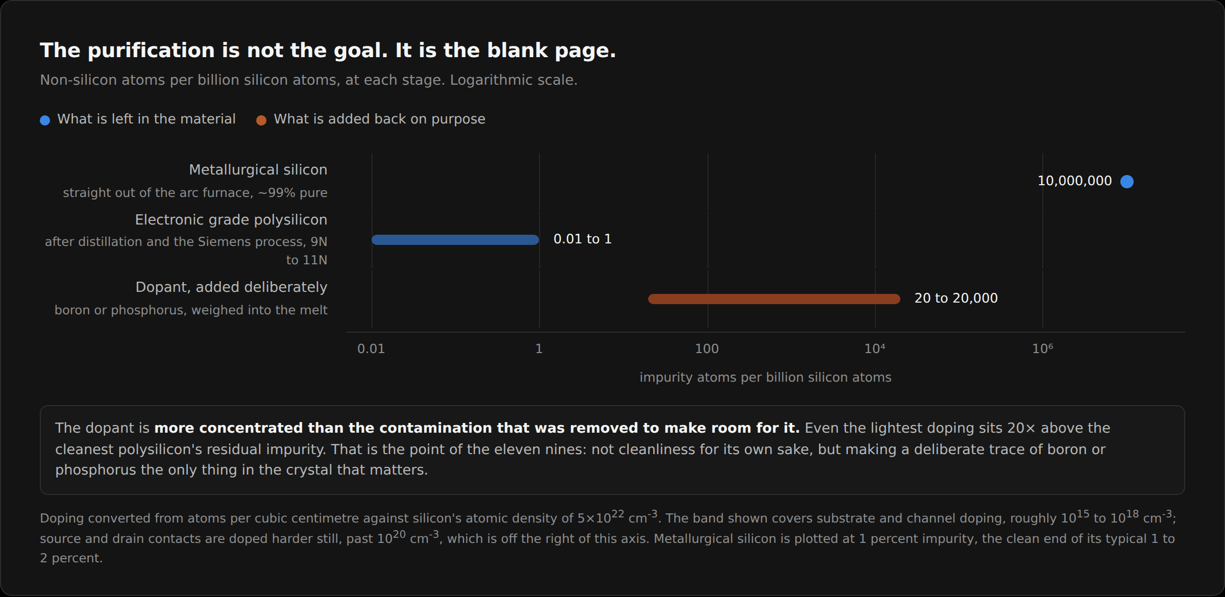
The dopant you add back is orders of magnitude more concentrated than the contamination you spent all that energy removing. The purification is not the goal. It is the blank page.
One crystal, not many
Polysilicon is pure, but it is polycrystalline. The "poly" is doing real work in that word: it is a jumble of small crystals fused together, each with its lattice pointing a different way.
Where two of those grains meet, the orderly lattice breaks. Those grain boundaries scatter moving charge carriers and trap charge, and two transistors built either side of one will not behave the same. At the scale modern devices are built, a boundary running through a transistor is not a defect you can tolerate. It is a different component.
So the polysilicon has to be rebuilt as a single continuous crystal, hundreds of millimetres across, with every atom in register.
The method is nearly a century old and is named after Jan Czochralski, who reportedly stumbled onto the principle in 1916 by dipping his pen into molten metal instead of his inkwell.
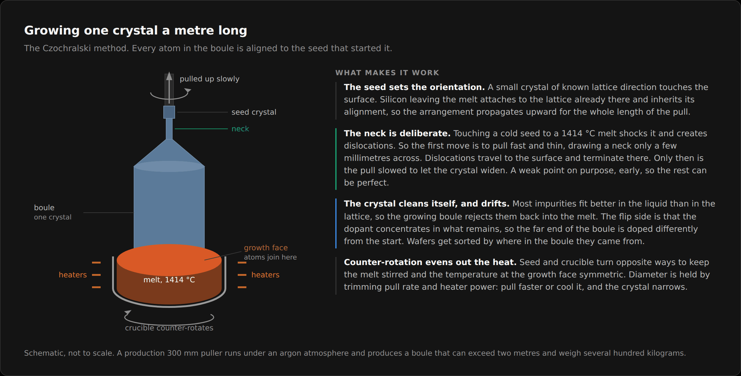
Polysilicon chunks are melted in a quartz crucible at a little over silicon's melting point of 1414 degrees Celsius. The dopant goes in here, weighed into the melt. A small seed crystal of known orientation is lowered until it just touches the surface, then drawn slowly upward while both seed and crucible rotate in opposite directions.
At the boundary between melt and solid, silicon atoms attach themselves to the existing lattice and inherit its alignment. Pull steadily and that alignment propagates upward for a metre or more.
Two details make this work that nobody mentions in the summary version.
The first is the neck. The initial contact between seed and melt creates dislocations from thermal shock. So the operator pulls fast for a while first, drawing out a thin neck only a few millimetres across, which lets those dislocations run out to the surface and terminate. Only then is the pull slowed to let the crystal widen into the full boule. A deliberate weak point, early, so the rest can be perfect.
The second is segregation. Most impurities fit better in the liquid than in the crystal lattice, so as the boule grows it rejects them back into the melt. The crystal purifies itself slightly as it goes. The flip side is that the dopant concentrates in the shrinking melt, so the far end of the boule is doped differently from the start, and wafers get sorted by where in the boule they came from.
From a cylinder to a mirror
What you have now is a silicon cylinder, potentially over two metres long and weighing hundreds of kilograms. It gets ground to an exact diameter, then sliced into wafers by a wire saw running diamond abrasive.
Then it gets lapped, etched, and polished, and the specification for that polish is the thing that stops people in their tracks. A finished wafer is flat to within a few tens of nanometres across its whole face.
Scaled up so that a 300 millimetre wafer covered an American football field, the highest hill on it would be roughly the thickness of a sheet of paper.
That is not showing off. Flatness is a photographic requirement, which is the next step.
Nothing is engraved
The word people reach for is engraving, and it is the wrong verb. Nothing is carved, scratched, or cut into the surface. The process is photography, run over and over.
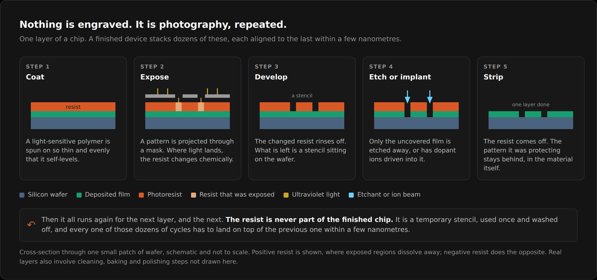
A layer goes like this. Coat the wafer in a light-sensitive polymer called photoresist, spun on so thin and even that it self-levels. Project an image of the desired pattern onto it through a mask, using ultraviolet light. Where light lands, the resist changes chemically and its solubility flips. Wash it, and the exposed regions (or the unexposed ones, depending on the resist) rinse away.
You are now left with a stencil made of hardened polymer, sitting directly on the silicon.
Then you do something through that stencil. Etch material away where the resist is not protecting. Or fire dopant ions at the wafer, which embed where they hit bare silicon and bounce off the resist. Or deposit a new film. Strip the resist off, and start the whole cycle again for the next layer.
A modern chip is dozens of these cycles stacked up, each aligned to the ones below it within a few nanometres. That alignment tolerance, called overlay, is as demanding as the printing itself.
Two things about this are worth knowing even at a light level.
You cannot easily print a feature much smaller than the wavelength of light you print it with, for the same reason you cannot paint a fine line with a fat brush. The industry ran deep ultraviolet at 193 nanometres for a very long time and printed features far smaller than that anyway, through a stack of tricks: flooding the gap with water to bend the light harder, deliberately distorting the mask so that diffraction pulls the projected image back into the shape you wanted, and printing a pattern in two or more passes that interleave.
Extreme ultraviolet, at 13.5 nanometres, is not simply a shorter wavelength. At that wavelength there is no such thing as a lens, because every known material absorbs it rather than transmitting it. The optics have to be mirrors, and the entire light path has to sit in vacuum, because air itself absorbs it too.
And the flatness matters because a projected image is only in focus over a very shallow depth. A bump on the wafer is a region that prints blurry.
Dicing and the package
The wafer is now a grid of finished but still-connected chips. They get electrically tested in place, the failures marked, and then the wafer is sawn or laser-cut into individual dies.
Not all of them work. Yield is the fraction that do, and it is governed largely by defects: a single stray particle landing in the wrong place during one of those dozens of photographic cycles can kill a die. This is the entire reason for cleanrooms, and it is another instance of the same theme. Keep things out.
There is also a loss that has nothing to do with defects at all, and it is pure geometry. The wafer is round and the chips are rectangles, so around the rim there is a ring of dies that fall partly off the edge. They are printed, they cost exactly as much to print, and they are scrap before the process even begins.
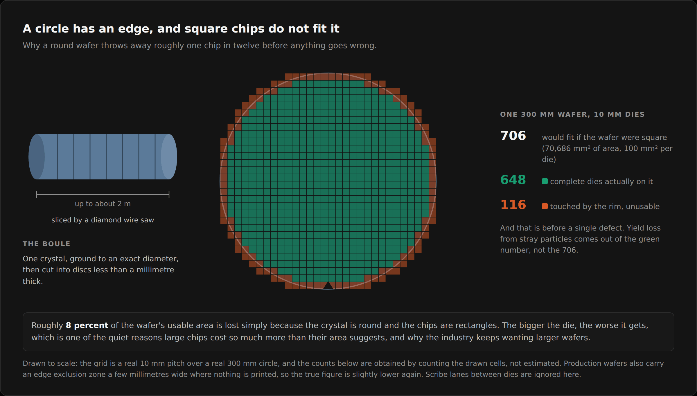
For a ten millimetre die the arithmetic is unforgiving: the wafer has enough area for about 706, but only 648 of them are actually whole. Roughly eight percent gone, and the larger the die the worse the ratio gets, which is a quiet part of why big chips cost so much more than their area suggests.
The working dies are mounted, connected out to pins or pads, and sealed into a package. The package is not decoration. It is mechanical protection, the path heat takes to get out, and the electrical bridge to the board, and if you have ever worked on a board you know that the package is where a lot of the real engineering constraints live.
What you have and what you do not
At the end of all of that you have a small slab of the purest material in industrial use, grown as one continuous crystal, polished flatter than almost anything else made, with a precisely measured amount of deliberate contamination patterned into it in a few dozen layers.
It does not compute anything. Nothing about it thinks. It is a very, very well organised rock.
It is worth seeing the whole chain on one scale before moving on, because the span is genuinely hard to hold in your head.
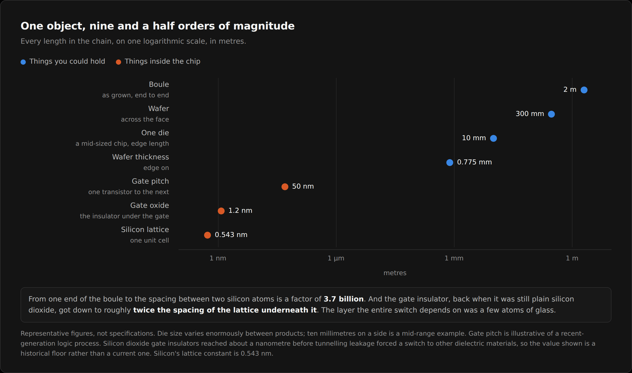
From one end of the boule to the gap between two silicon atoms is a factor of 3.7 billion. And the last two rows are where part two lives: the gate insulator, back when it was still ordinary silicon dioxide, came down to roughly twice the lattice spacing of the crystal underneath it. The layer that the entire switch depends on was a few atoms of glass, and it works because it does not conduct.
Part two is about the step that makes it a machine: how a boundary between doped regions becomes a switch, how a few switches become arithmetic, and how that climbs, layer by layer, all the way up to a program running inside a sandbox that is trusting every single one of these layers to hold.
Climb it in GregTech
GregTech, a tech mod for Minecraft, makes its silicon chips the same way this part does. In the TerraFirmaGreg modpack you grow a silicon seed crystal, pull a boule out of molten polysilicon, and cut it into wafers. The ladder below starts there, on the sand rung, and climbs one tier at a time through the steps in part two.
Gunnar
Founder, Tofte Ventures LLC